


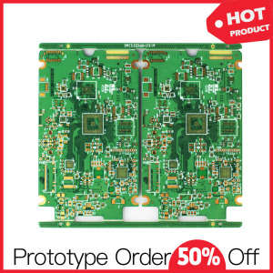


Only do quick turn of quality PCB circuit boards.
NOD Electronic focus on quick turn of quality PCB circuits, including multilayer PCB, FPC, HDI, impedance, blind & buried vias etc. and deliver outstanding services.
PCB Circuit Manufacturing Capabilities
| Total Pad Size | Standard | Advanced |
| Capture Pad | Drill + 0.008 | Drill + 0.006 |
| Landing Pad | Drill + 0.008 | Drill + 0.006 |
| BC Mechanical Drill (Type III) | 0.008 | 0.006 |
| Laser Drill Size | 0.004-0.010 | 0.0025 |
| Material Thickness | 0.0035 | 0.0025 |
| Stacked Via | Yes | Yes |
| Type I Capabilities single & Double Deep | Yes | Yes |
| Type II Capabilities Buried Vias with Microvias | Yes | Yes |
| Type III Capabilities | Yes | Yes |
| Copper Filled Microvia | Yes | Yes |
| Smallest Copper Filled Microvia | 0.004 | 0.0025 |
| Copper Filled Microvia Aspect Ratio | 0.75:1 | 1:01 |
| Smallest Laser Microvia Hole Size | 0.004 | 0.0025 |
| Laser Via Aspect Ratio (Depth:Diameter) | 0.75:1 | 1:01 |
PCB Circuit Manufacturing Process

Who We Are
As a service-leading custom PCB circuit manufacturing and PCB assembly (PCBA) partner, NOD Electronics strives to support international small-medium business with 10+ years engineering experience in Electronic Manufacturing Services (EMS). Our headquarter is located in Guangzhou, China. We have 10,000 square meters plant, 287 employees and 42 engineers, monthly capabilities of 15,000 square meters PCB design & fabrication and 80 million spot SMT. We were approved by ISO9001-2008, TS16949, UL, CE, RoHS.
Our customers are widely distributed in mainland China, Taiwan, the United States, Japan, Singapore, Korea, Russia, Germany, Switzerland and other parts of the word.
